
## Le défi de l'effondrement de tension dans l'alimentation électrique des GPU d'IA
Les accélérateurs IA modernes—en particulier les GPU haut de gamme utilisés dans les clusters d'entraînement—reposent sur une mise à l'échelle de tension de plus en plus agressive pour maximiser l'efficacité des transistors et la marge thermique. Leurs dispositifs de positionnement de tension (VPD) et leurs PMIC fonctionnent désormais à des rails nominaux aussi bas que 0,35 V, avec des exigences de creux dynamique descendant sous 0,25 V pendant les transitoires de plusieurs kA. Ces conditions exposent une lacune critique dans les tests de charge électronique CC conventionnels : la plupart des charges perdent leur régulation, leur précision, voire leurs fonctionnalités de base sous 0,5 V, en particulier lors de l'absorption de >1 kA.
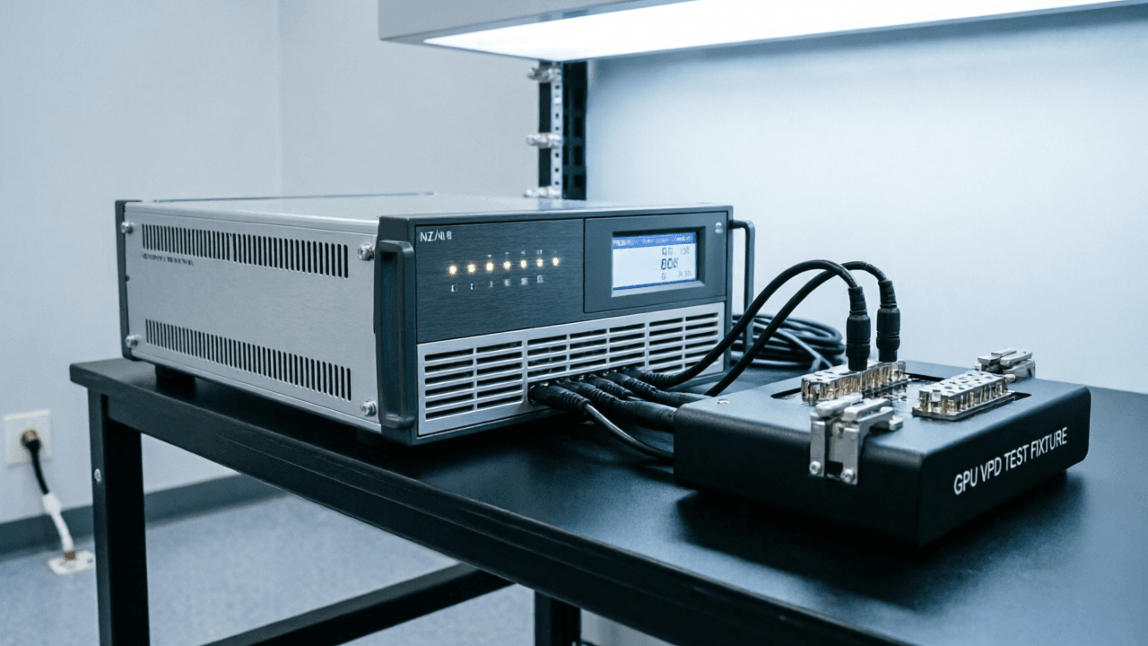
Les charges standard spécifient généralement des tensions de fonctionnement minimales de 0.8–1.0 V à plein courant — et beaucoup ne peuvent maintenir la régulation en dessous de 0.6 V sans erreur significative ni instabilité. Pourtant, les scénarios de test de charge à ultra basse tension GPU VPD nécessitent une charge précise et répétable jusqu'à 0.2 V à des courants allant jusqu'à 5000 A. Sans cette capacité, les ingénieurs ne peuvent pas vérifier la réponse transitoire, la stabilité de la boucle ou la récupération de l'affaissement sous des profils de charge de travail IA réels.
## Pourquoi les charges standard défaillent en dessous de 0.5 V
Les charges électroniques conventionnelles utilisent des architectures à base de MOSFET optimisées pour les applications à tension plus élevée et à courant plus faible. Lorsque la tension chute, les pertes de conduction augmentent de manière quadratique, et les marges de commande de grille se réduisent—ce qui entraîne un emballement thermique, des oscillations ou un arrêt brutal. De plus, la mesure de courant basée sur un shunt devient imprécise à des tensions ultra-faibles en raison des limitations du plancher de bruit et des interférences de chute de tension IR. Même les charges actives de précision manquent souvent de la marge de tension faible *et* de la densité de courant élevée nécessaires simultanément.
La validation VPD des GPU exige les deux extrêmes : un contrôle de tension rigoureux (±1 mV) à <0,3 V *tout en* absorbant 3–5 kA par paliers de <10 µs. Il ne s'agit pas simplement de mettre à l'échelle le matériel existant — il faut repenser de fond en comble la topologie de l'étage de puissance, la gestion thermique et l'architecture de rétroaction.
## NZ/N Series : Conçu pour la réalité Sub-0.5V, Multi-kA
La charge électronique CC à ultra-basse tension et courant élevé de la série NZ/N est spécialement conçue pour ce régime précis. Ses spécifications sont définies par des limites physiques — et non par des seuils marketing : **–2.4 V @ 1200 A** et **0.2 V @ 5000 A**, vérifiées sur l'ensemble de son domaine de fonctionnement. Contrairement aux conceptions dérivées ou modifiées, la série NZ/N utilise une architecture synchrone brevetée à faible VDS(on) avec une gestion thermique répartie et une compensation adaptive de commande de grille — permettant un fonctionnement stable et immunisé contre le bruit à la limite de la physique du silicium.
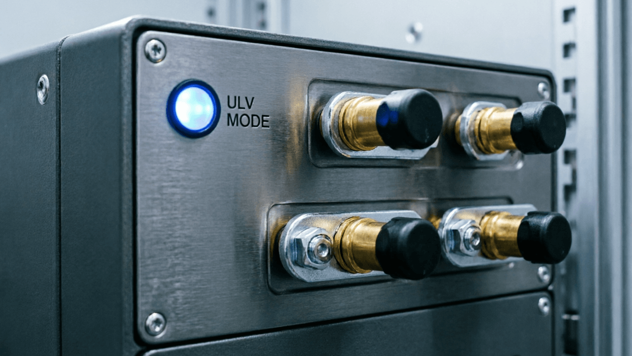
Cette capacité permet directement des flux de travail de test de charge à ultra basse tension GPU VPD réalistes — y compris des paliers de charge dynamiques, des transitoires à slew rate contrôlé et un vieillissement de longue durée sur des rails nominaux de 0.25 V. Elle prend en charge la validation du système complet à travers les phases de R&D, de tests de production ATE, de vieillissement de fiabilité et de certification — dans le cadre de la [GPU PMIC Test Solution](/solutions/gpu-pmic-test-solution) intégrée.
## Au-delà des fiches techniques : l'adéquation à l'application compte
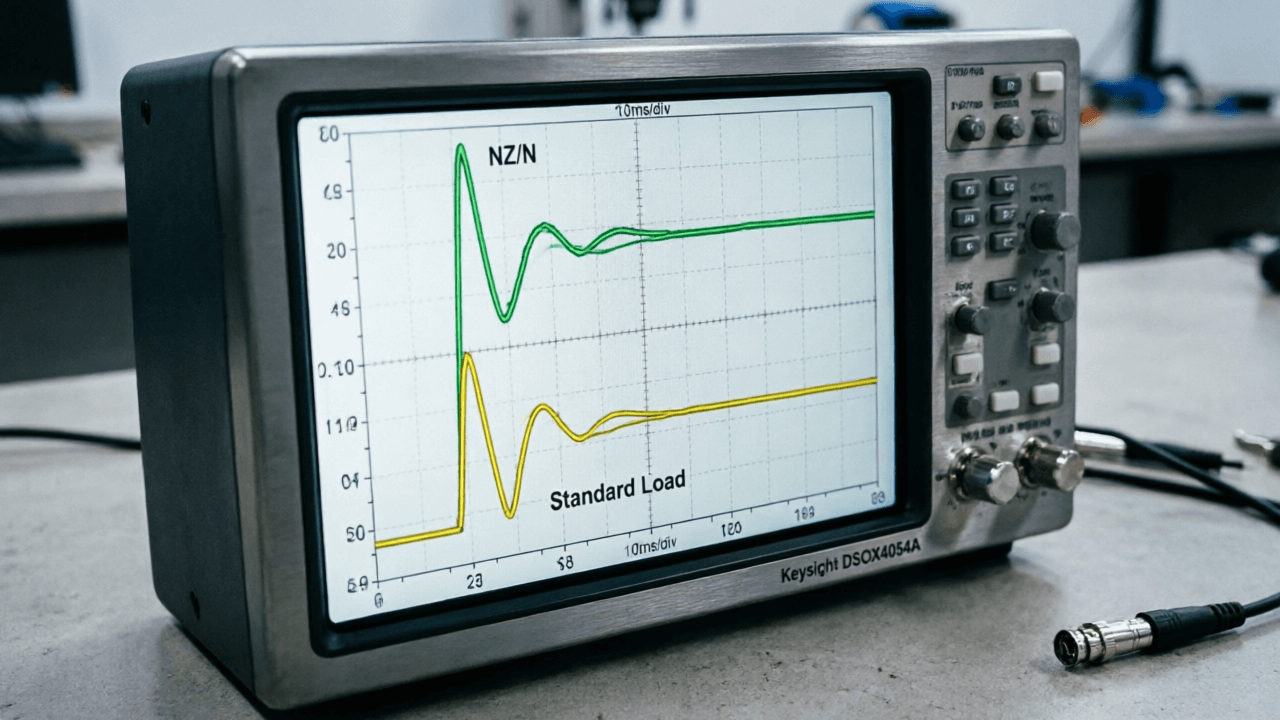
Le choix d'une charge ne consiste pas simplement à atteindre un seuil de valeur de tension. Il s'agit de maintenir la bande passante, la linéarité et la répétabilité *sur* toute cette bande de basse tension. La série NZ/N y parvient grâce à une détection de courant conçue conjointement (utilisant des shunts à connexion Kelvin compensés en température), à un réglage PID adaptatif par plage de tension et à une correction d'offset de zéro tension calibrée par firmware. Ces caractéristiques garantissent qu'une charge échelonnée de 0,2 V, 4000 A produit des formes d'onde propres et mesurables — sans oscillations, dépassement ni artefacts de décrochage qui masqueraient le comportement réel du VPD.
Pour les équipes développant la distribution d'alimentation des GPU de nouvelle génération, le choix ne se pose pas entre « suffisant » et « idéal »—il s'agit de choisir entre *vérité mesurable* et *hypothèse non vérifiée*. Lorsque votre VPD doit réguler à ±3 mV près à 0,28 V sous des transitoires de 4,2 kA, seules les charges conçues avec la même exigence extrême—comme la [charge électronique DC à très basse tension et courant élevé de la série NZ/N](/products/dc-electronic-load/nz-n-series-ultra-low-voltage-and-high-current-dc-electronic-load)—offrent la fidélité requise pour l'assurance de l'intégrité d'alimentation à l'échelle de l'IA.

FaithTech
FaithTech conçoit et fabrique des alimentations électriques à courant continu programmables et des charges électroniques pour les secteurs de l’énergie, de l’industrie, de l’automobile, de l’électronique et de l’aérospatiale.
Tous droits réservés © 2026 FaithTech